✍️ [#02] 왜 반도체는 실리콘을 사용할까? (Semiconductor Manufacturing Process: Why Silicon Dominates)
— 모래에서 시작되는 첨단 산업
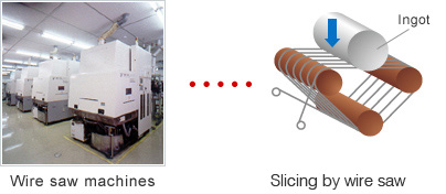
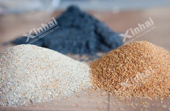


📌 오늘의 범위
- 반도체 재료 개요
- 실리콘 정제 과정
- 단결정 성장 기초
🚀 핵심 요약
- 실리콘은 지구에서 매우 풍부하다
- 열/화학적 안정성이 뛰어나다
- 초고순도 정제가 가능하다
👉 “산업적으로 가장 완성된 재료”
📊 반도체 재료 분류
[Semiconductor Materials]
 ├─ Elemental
 │   ├─ Silicon (Si)
 │   └─ Germanium (Ge)
 │
 └─ Compound
     ├─ GaAs
     ├─ GaN
     └─ SiC
👉 현실:
90% 이상 = Silicon
🔍 왜 하필 실리콘인가?

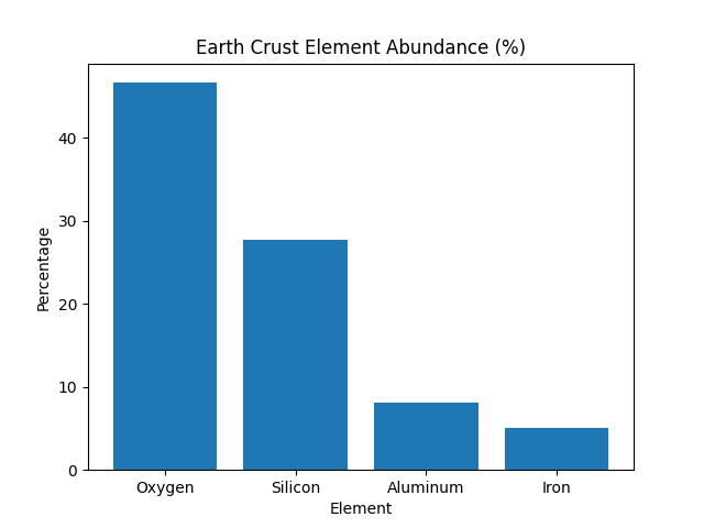
실리콘은 지각에서 산소 다음으로 풍부하다
이걸 산업적으로 해석하면:
1️⃣ 공급 안정성
- 원재료: SiO₂ (모래)
- 거의 무한 공급
👉 생산량 제한 없음
👉 가격 안정성 확보
2️⃣ 공정 적합성 (가장 중요)
실리콘의 결정적 장점:
👉 SiO₂ (산화막) 형성 가능
📊 실리콘의 공정 핵심 구조
[Silicon (Si)]
     ↓ 산화
[SiO₂ Layer]
     ↓
 ├─ 절연층
 ├─ 게이트 산화막
 └─ 보호막
👉 핵심:
산화막이 반도체 공정의 시작과 끝
3️⃣ 고순도 정제 가능
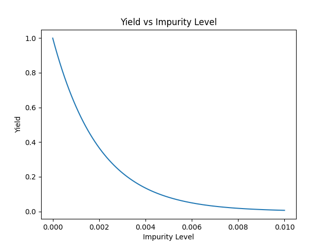
반도체는 “순도 싸움”이다
👉 불순물 = 불량
⚙️ 실리콘 제조 과정
🖼️ 정제 → 잉곳 → 웨이퍼
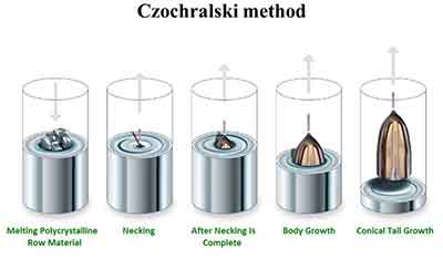
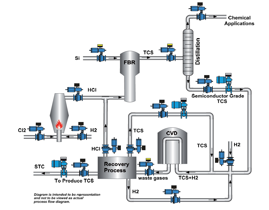

📊 실리콘 정제 프로세스
SiO₂ (모래)
   ↓ (탄소 환원)
Si (저순도)
   ↓ (염화 반응)
SiHCl₃ / SiCl₄
   ↓ (정제 / 증착)
High Purity Si
👉 결과:
99.999999% 이상 순도 필요
⚙️ 엔지니어 관점 해석
여기서 중요한 건 하나:
👉 “좋은 재료”가 아니라
👉 “공정에 최적화된 재료”
📊 반도체 재료 선택 기준
[Material Selection Criteria]

 ├─ Thermal Stability
 ├─ Chemical Reactivity
 ├─ Purification Capability
 └─ Supply Scalability
👉 실리콘은 이걸 모두 만족
🏭 실제 FAB 관점
✔ 재료 변경이 의미하는 것
- 공정 조건 전부 변경
- 장비 재설계 필요
- 수율 급락
👉 즉:
“재료 변경 = 산업 리셋”
✔ 그래서 생기는 현실
- Silicon → 주류
- GaN / SiC → 특정 영역만
💡 한 줄 인사이트
👉 실리콘은 최고의 재료가 아니라
“가장 최적화된 생태계”다
🎯 다음 글 예고
👉 “단결정은 왜 필요한가?”
— CZ vs FZ 완전 해부
✍️ [#02] Why Silicon?
— From Sand to Semiconductor
🖼️ Cover Image
(Use the same image above)
📌 Scope
- Semiconductor materials
- Silicon purification
- Basics of crystal growth
🚀 Key Summary
- Silicon is abundant
- Thermally and chemically stable
- Can be purified to ultra-high levels
👉 “The most industrially optimized material”
📊 Diagram 1: Material Types
[Semiconductor Materials]
 ├─ Elemental
 │   ├─ Silicon
 │   └─ Germanium
 │
 └─ Compound
     ├─ GaAs
     ├─ GaN
     └─ SiC
🔍 Why Silicon?
Silicon is the second most abundant element in Earth’s crust
1️⃣ Supply Stability
- Raw material: sand
- Virtually unlimited
2️⃣ Process Compatibility
👉 Key advantage:
Forms stable SiO₂ layer
📊 Diagram 2: Core Mechanism
[Silicon]
   ↓ Oxidation
[SiO₂ Layer]
   ↓
 ├─ Insulator
 ├─ Gate oxide
 └─ Protection
3️⃣ High Purity Capability
👉 Impurities = defects
📊 Diagram 3: Purification Flow
SiO₂
 ↓
Si
 ↓
SiHCl₃
 ↓
Ultra Pure Si
⚙️ Engineering Insight
👉 Silicon is not just “good”
👉 It is process-optimized
📊 Diagram 4: Selection Criteria
[Material Criteria]

 ├─ Thermal Stability
 ├─ Chemical Control
 ├─ Purification
 └─ Scalability
🏭 FAB Perspective
Changing material means:
- Redesign processes
- Rebuild equipment
- Yield collapse
👉 Hence:
Silicon dominance
💡 Insight
👉 Silicon is not the best material,
but the most optimized ecosystem
🎯 Next Episode
👉 “Why Single Crystal?”
— CZ vs FZ deep dive
'Semiconductor' 카테고리의 다른 글
| [#04] 웨이퍼는 왜 둥글까? (0) | 2026.04.14 |
|---|---|
| [#03] 왜 반도체는 ‘단결정’이어야 할까? (0) | 2026.04.07 |
| [#01] 반도체는 왜 세상을 지배하는가 (0) | 2026.04.07 |
| [#00] Index - 반도체 공정, 장비 기초 (0) | 2026.04.07 |
| HBM 시대, 반도체 물류자동화의 승자는 누구인가? (0) | 2026.03.27 |


